



Contact Us
Looking for customized wafer fabrication equipment for your wet wafer processing, ECP, Furnace, Track and SFP?
Let’s ConnectAdvanced IC manufacturing, wafer-level packaging, and compound semiconductor production all share a vital processing requirement: the use of wet processing for critical removal and additive steps, including precision wafer cleaning, etch, photoresist strip, metal lift-off, coating, and developing.
ACM Research develops and delivers high-performance wet process equipment—including advanced single-wafer cleaning systems and highly configurable semiconductor wet benches—engineered to support the industry’s most demanding logic, memory, and advanced packaging applications. Our wet processing tools combine chemical efficiency, process precision, intelligent automation, and proven sustainability advantages to help manufacturers achieve contaminant-free surfaces, tighter process control, and consistently higher yields.
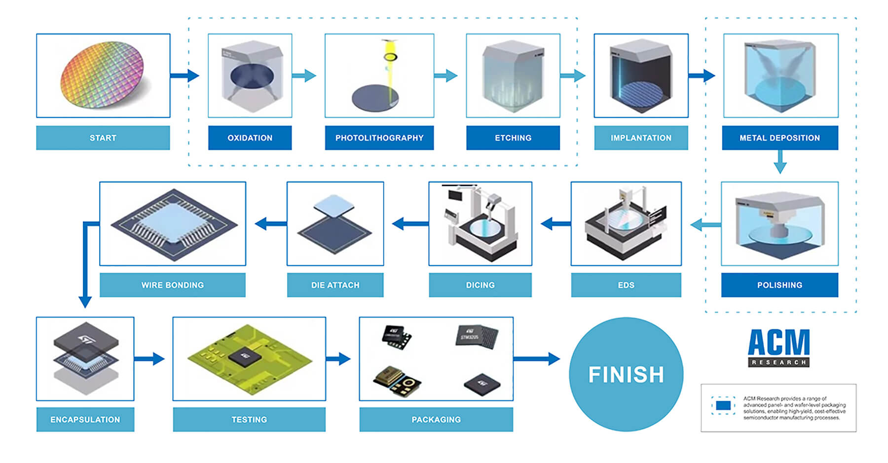
Creating a semiconductor requires several hundred cleaning and surface preparation steps, numerous photoresist stripping variations to remove patterning film layers, and a wide range of etch processes to form patterns, create vias, and prepare surfaces for deposition.
As device geometries shrink and integration requirements intensify, manufacturers need wet processing solutions that deliver exceptional cleanliness, uniformity, and reliability—without compromising productivity or chemical consumption. ACM’s proprietary process technologies and next-generation wet processing systems are designed to meet these challenges head-on, helping customers build high-yield, power-efficient, and cost-effective microelectronics for advanced nodes.
Download Technical Paper: High Performance, Eco-Friendly SPM Cleaning Technology using Integrated Bench-Single Wafer Cleaning System
Download Technical Paper: Development and Application of BEOL Polymer Residue Removal Technology
Download Technical Paper: Stripping Process Development using SAPS Megasonic Technology
Download Technical Paper: TSV Cleaning Using SAPS™ Megasonic Cleaning Technology
Read Blog: Cleaning Challenges and Solutions for 3D Memory and NAND
Read Blog: ACM’s SAPS Technology Optimizes Single-Wafer Cleaning
Looking for customized wafer fabrication equipment for your wet wafer processing, ECP, Furnace, Track and SFP?
Let’s Connect